草草影院ccyy,妖精漫画免费登录页面入口大全 ,国产成人a亚洲精品无码青草,嫩草欧美一二三四

SOI FAB SOI TECH  |  SOI APP  |  SOI FAB  |  SOI SPECS  |  SOI ADVA.
As a world leading player in fabrication of SOI materials, Simgui adopts 4 methods to provide a wide range of SOI products.


[Click to zoom]
1. SIMOX


SIMOX, which stands for Separation by Implantation of Oxygen, is a process that Simgui uses to create an insulating layer between the layers of a bulk silicon wafer. There are two essential stages of the process: ion implantation and annealing.
In the implantation stage, oxygen ions are implanted in the silicon wafer and react with the silicon to form silicon dioxide precipitates. However, the implantation causes considerable damage to the wafer and the layer of silicon dioxide precipitates is not continuous. Thus high-temperature annealing helps repair the damage and form the oxide precipitates into a continuous layer. Now the silicon's quality is restored and the buried oxide (BOX) layer can act as a highly effective insulator.


[Click to zoom]
2. Bonding


By using bonding chemistry between silicon (Si) and silicon dioxide(SiO2) or between SiO2 and SiO2 effectively, two Si wafers are tightly bonded with a SiO2 layer as an insulator inside the bonded pair. After one side of the Si bulk is thinned down properly with a desired active Si layer thickness, bonded SOI wafers are obtained.
The fabrication process is accomplished by three basic steps. The first step is to mate a thermally oxidized wafer on a non-oxidized wafer at room temperature. The second step is to anneal the bonded pair to increase bonding strength. The third step is to thin down one side of the bonded pair to an appropriate thickness by grinding, etching and polishing.


[Click to zoom]
3. Simbond


Derived from conventional wafer bonding and ion-implantation technologies comes another method called Simbond that Simgui originates in preparation of SOI materials.
The ion-implantation provides a well distributed ion-implanted layer. This layer serves as a chemical etch stop layer, which allows for an excellent uniformity control on the thickness of the device layer before a final polish process. The innovated process can produce high quality SOI wafer with superior SOI uniformity and thick BOX layer.


Top
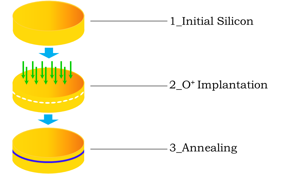
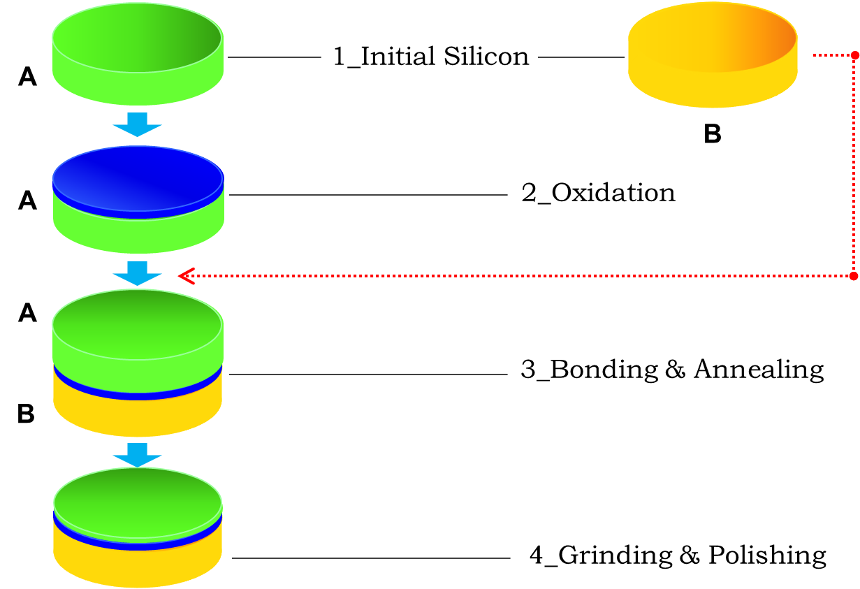
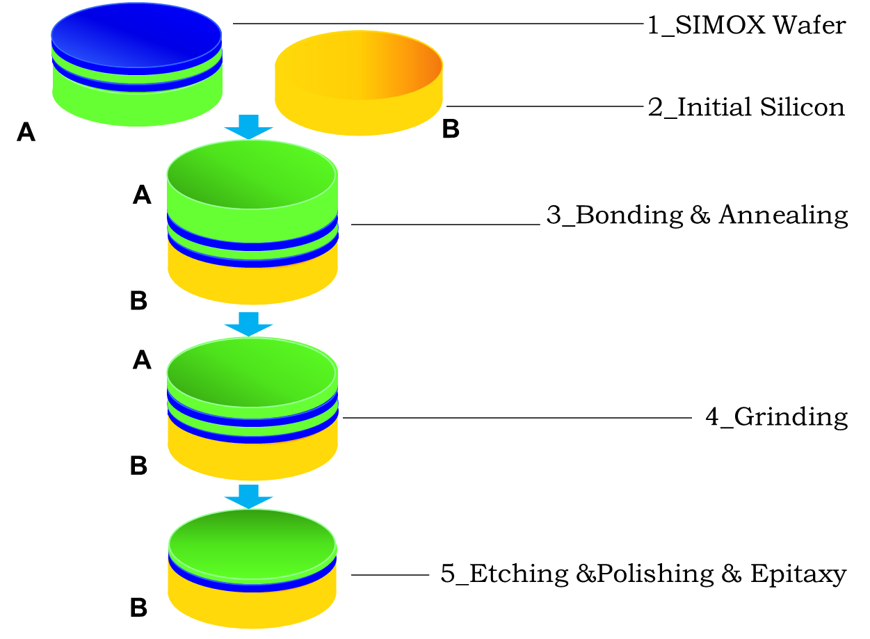
Simgui adopts four processes: SIMOX, BONDING, SIMBOND, and SSS, and uses advanced equipment to prepare SOI materials to ensure that wafers can meet international semiconductor standards and meet the requirements of mainstream IC production lines in the world today. Relying on strong and continuous technical support, integrating the good cost-effectiveness of domestically produced substrates and the advantages of strong and flexible processing capabilities, we provide professional epitaxial services to customers.
Address: 200 Xinlai Road, Jiading District Shanghai 201815, PRC Tel: +86-21-6952 2599 Fax: +86-21-6952 2221
主站蜘蛛池模板: 聂荣县| 普兰店市| 平遥县| 红安县| 台南县| 拜泉县| 凤冈县| 叶城县| 习水县| 金昌市| 大新县| 乌拉特中旗| 新丰县| 崇礼县| 根河市| 依安县| 鄂尔多斯市| 滁州市| 共和县| 鄂托克前旗| 明光市| 灵寿县| 吐鲁番市| 乌兰浩特市| 龙游县| 古浪县| 宜昌市| 孝义市| 邛崃市| 河曲县| 中宁县| 北京市| 许昌县| 元谋县| 达尔| 阳曲县| 紫阳县| 皋兰县| 赣州市| 萝北县| 会泽县|